Globally unique combination paves the way for advanced characterization techniques for magnetic materials or spintronic devices
Next generations of spintronic devices, such as magnetic random access memory and high-frequency microwave generators, will require small dimensions, but also versatile functionalities. This involves challenging requirements for nanofabrication and, increasingly, also for high-accuracy measurement techniques.
To tackle these complex challenges, Raith and IOPCAS succeeded in organically merging an in-situ DC and high frequency magnetotransport measurement system, by incorporating an electromagnet in an electron beam lithography system with high resolution. The device meets the stringent requirements of advanced R&D in nanosized spintronics.
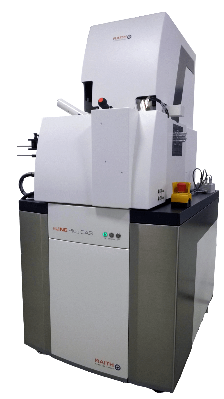
These combined functions create a globally unique workflow, hosted by the eLINE Plus Nanoengineering workstation. This new system, ![]() , is named after the hosting subsystem and Raith’s development partner for this new product, The Institute of Physics, Chinese Academy of Science (CAS).
, is named after the hosting subsystem and Raith’s development partner for this new product, The Institute of Physics, Chinese Academy of Science (CAS).
Efficient sample characterization and development
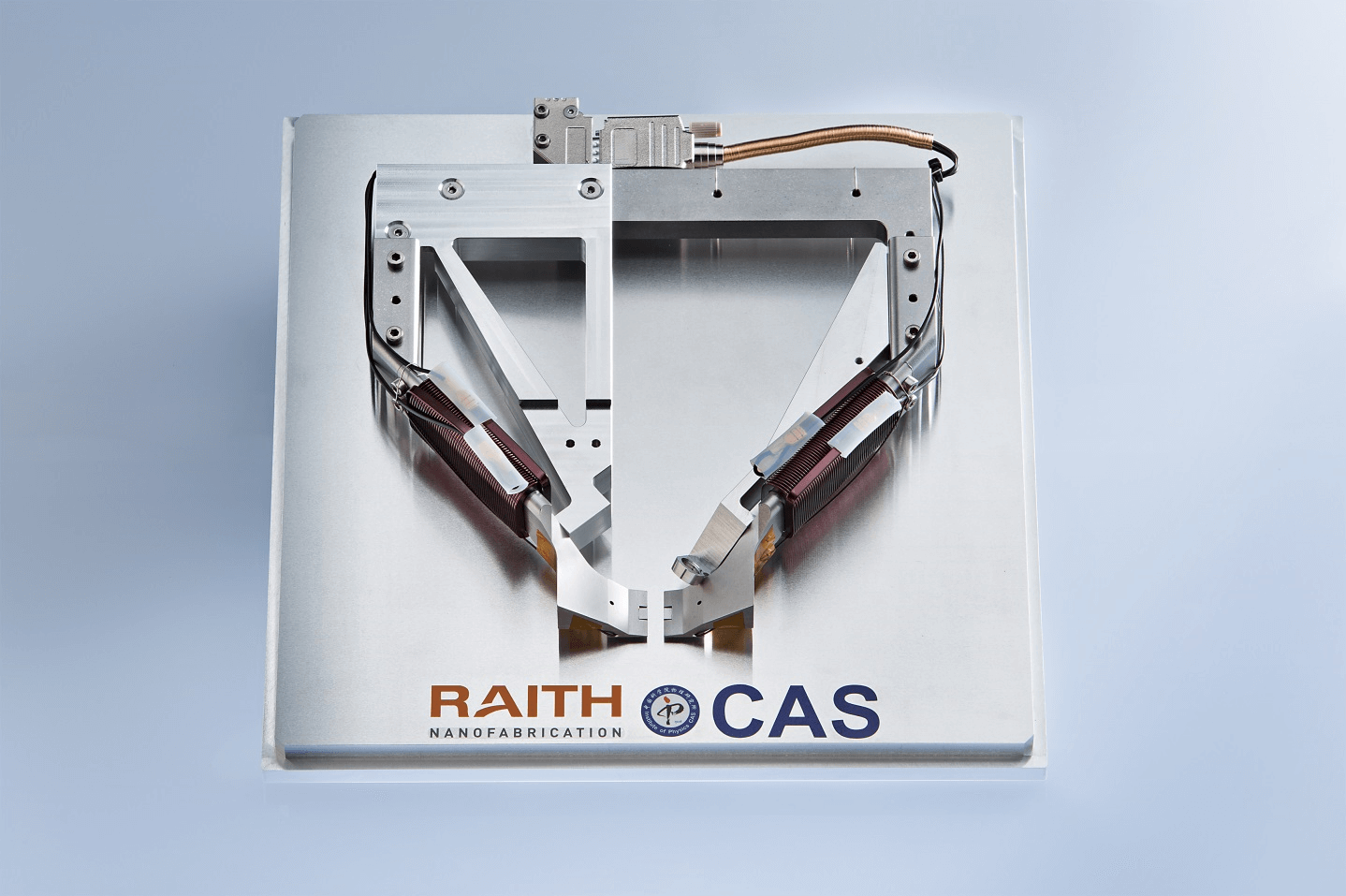
The patented design of the MYA allows extremely confined, local and homogenous magnetic (4x4mm², <1% dev, up to 300 Oe.) and electrostatic fields to be applied exclusively at the plane of the sample surface.
To avoid interference of the MYA assembly with the EBL and SEM imaging capability of the eLINE Plus, the assembly can be fully retracted from its working position underneath the electron optics pole piece in seconds without breaking the vacuum.
The measurement and characterization of a magnetic device can be done by hardwired sample, but also by using up to 4 nano probers (ordered separately). With the help of the electron beam in imaging mode, the prober heads can be placed on contact pads while the MYA is its working position. Two out of the four prober heads can carry high frequency probers (40 GHz).
Measuring the in-situ transport property of a small magnetic tunnel junction
As one example from the wide field of applications, in-situ transport property of a small magnetic tunnel junction was measured. The magnetic tunnel junction is composed of two ferromagnetic layers interspersed by one insulating barrier layer (Figure 3a). The longitudinal resistance of the device is related to the magnetic structure of the two ferromagnetic layers, with their parallel and antiparallel alignment of magnetizations leading to low and high resistances respectively. Figure 3b shows the acquired character of the resistive behavior of the junction. The magnetic field was changed back and forth between a parallel and antiparallel state by changing the current through the coils, demonstrating the effectiveness of the magnet.
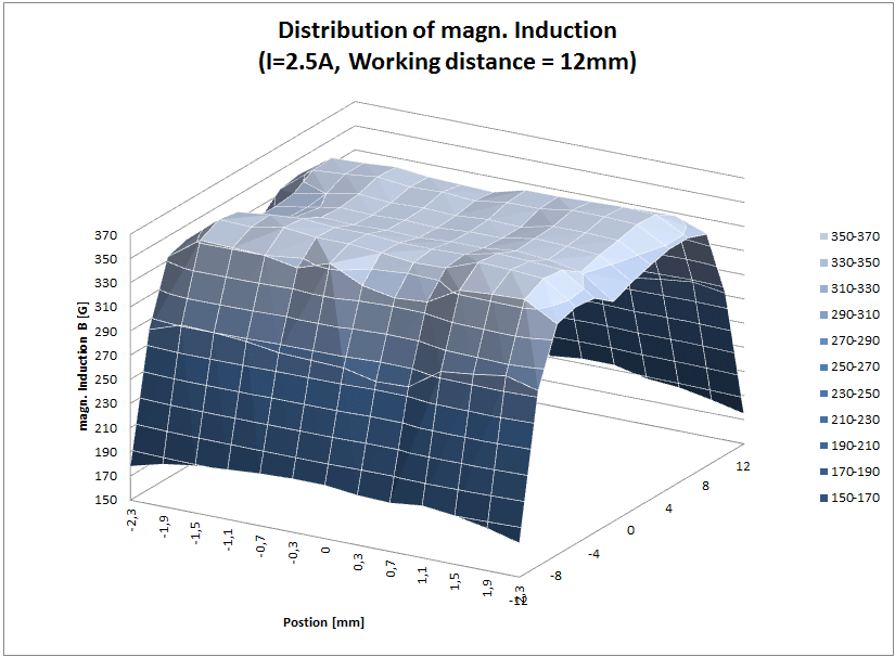
Figure 3: Field distribution in the plane of sample holder. Region with uniform field (<1% dev) reaches about 4mm×4mm.
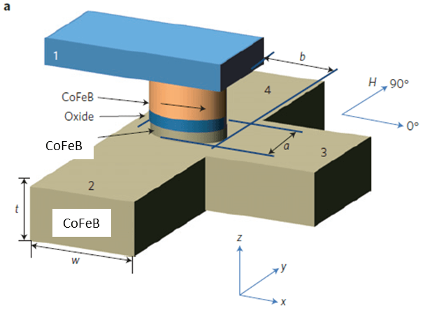
Figure 3a
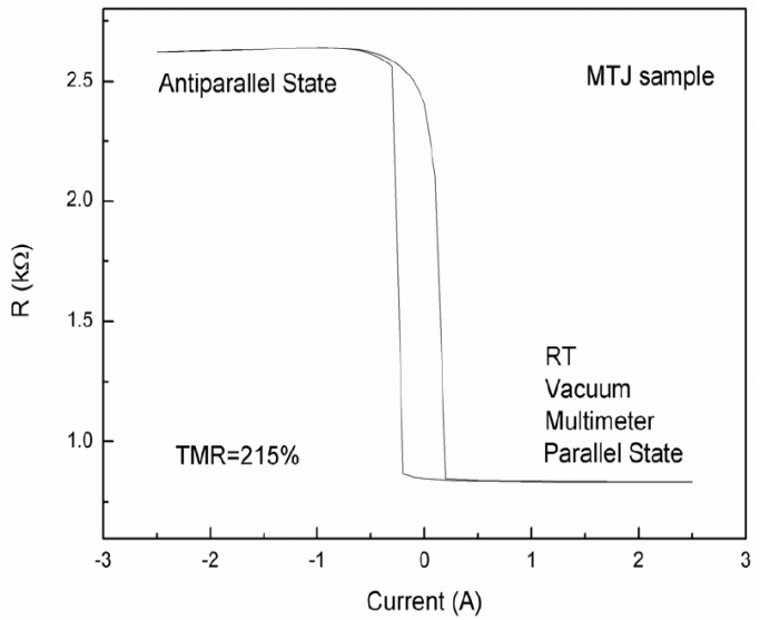
Figure 3b
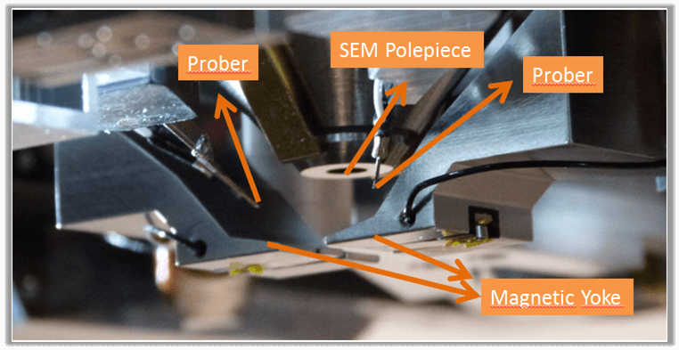
Figure 5: Integration and working position of magnetic yoke assembly and two DC probers in the vacuum chamber underneath the e-beam pole piece
Combining a magnetic field with ordinary EBL or SEM not only provides magnetoelectric measurement capability, but also sheds light on the hybridization of SEM with a magnetic force microscope or magneto-optical Kerr microscope, thus advancing the development of characterization techniques for magnetic materials or spintronic devices.
Are you interested in this topic, or do you have any further questions? Don’t hesitate to get in touch with our Sales Manager at sales@raith.com and find out how we can help you with your nanofabrication needs.