Review paper available: Comparison of technologies for nano device prototyping with focus on ion beams
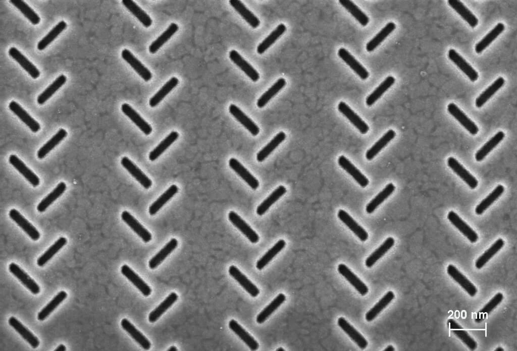
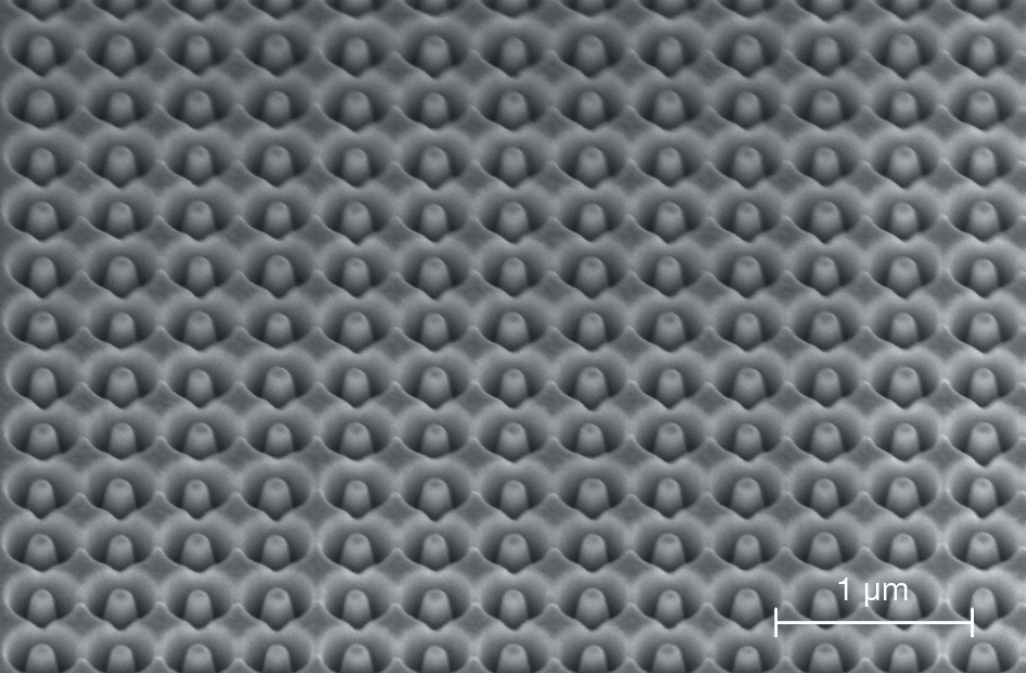
Nano devices are becoming increasingly important in various disciplines such as electronics, optics medicine, etc. But before they can be made available in or as commercial products, prototypes need to be manufactured to realize and asses ideas and theories for the final nano device. For those prototypes often very different approaches are necessary than in the final nano device fabrication. A review by Dr. Lars Bruchhaus et al. compares the four most common techniques used for nano device prototyping (NDP), electron beam lithography, self-organized 3D epitaxy, atomic probe microscopy and ion beam techniques. A focus is put on the latter while taking a closer look on ion beam techniques based upon liquid metal (alloy) ion sources, as recent developments have significantly increased their applicability for NDP. The review was recently published by the American Institute of Physics (AIP). To read the whole article, please download it here:
A German summary can also be found here.