Overcoming the limitations of nanofabrication – New white paper available
Today’s nanofabrication applications are mainly served by electron beam lithography, which allows wafer scale patterning down to nanometer accuracy in terms of placement and feature size within a reasonable time. But this technology also has its downsides: EBL must be combined with other techniques used in the process chain, and furthermore, patterning is limited to lithography on flat surfaces.
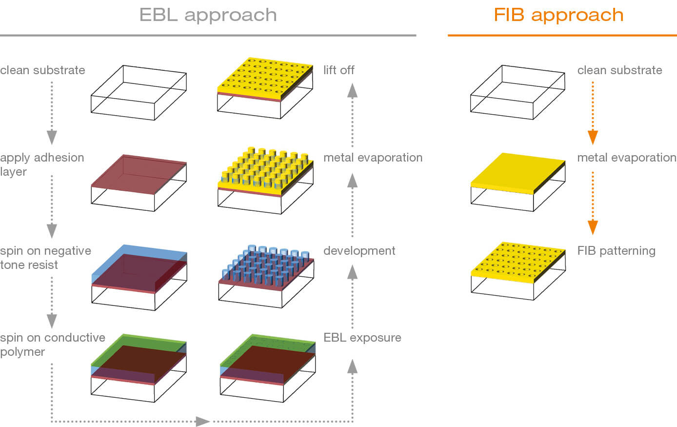
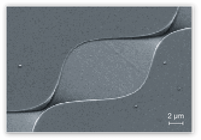
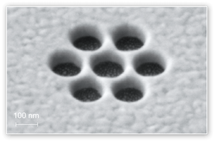
Those downsides can be circumvented by using a FIB-SEM which is optimized for nanofabrication. 3D patterning, even over topographic samples, and fewer process steps through the resistless fabrication method are just two of the benefits of using a focused ion beam for nanofabrication.
Our newest white paper highlights the advantages of using a FIB-centric FIB-SEM for nanofabrication of various application examples. Learn how applications such as 3D nanostructures at once-over-mm length, FIB hard masking of large area patterns, and many more can be addressed with our new FIB-SEM VELION and download the Whitepaper here: