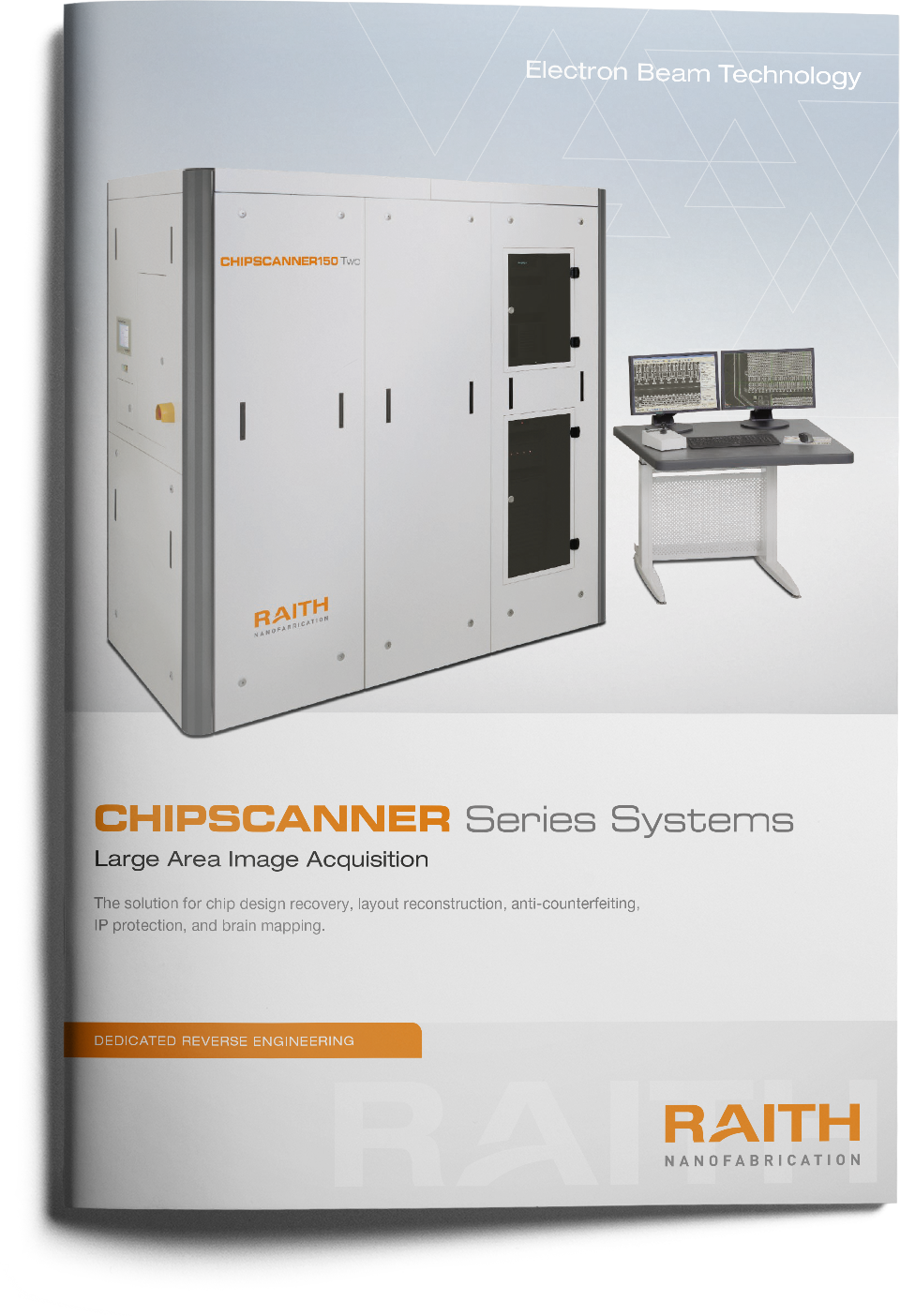
Large Area Image Acquisition
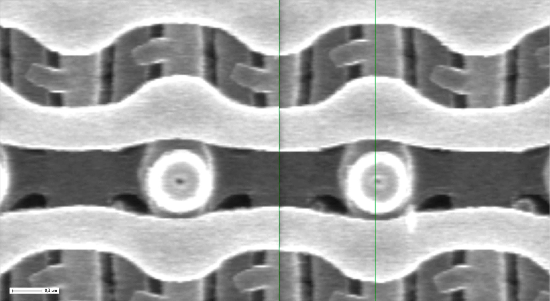
3D SEM image mosaics stitched over large areas and in 3D with CAD shape extraction
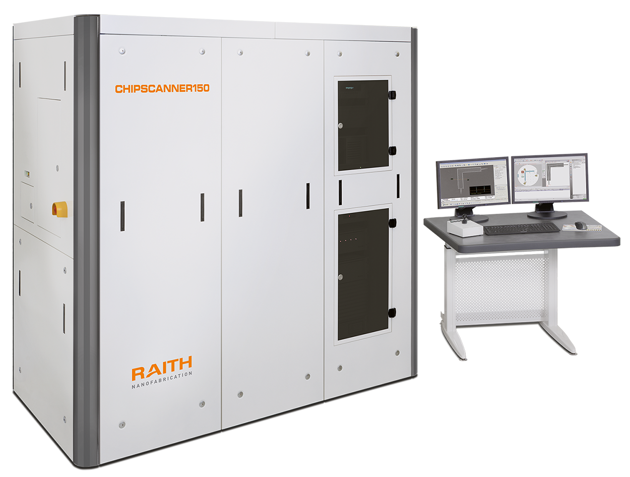
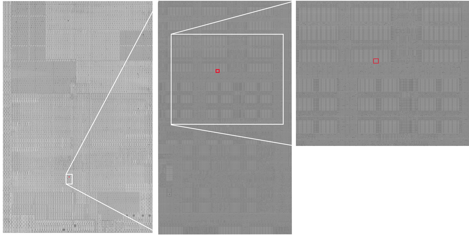
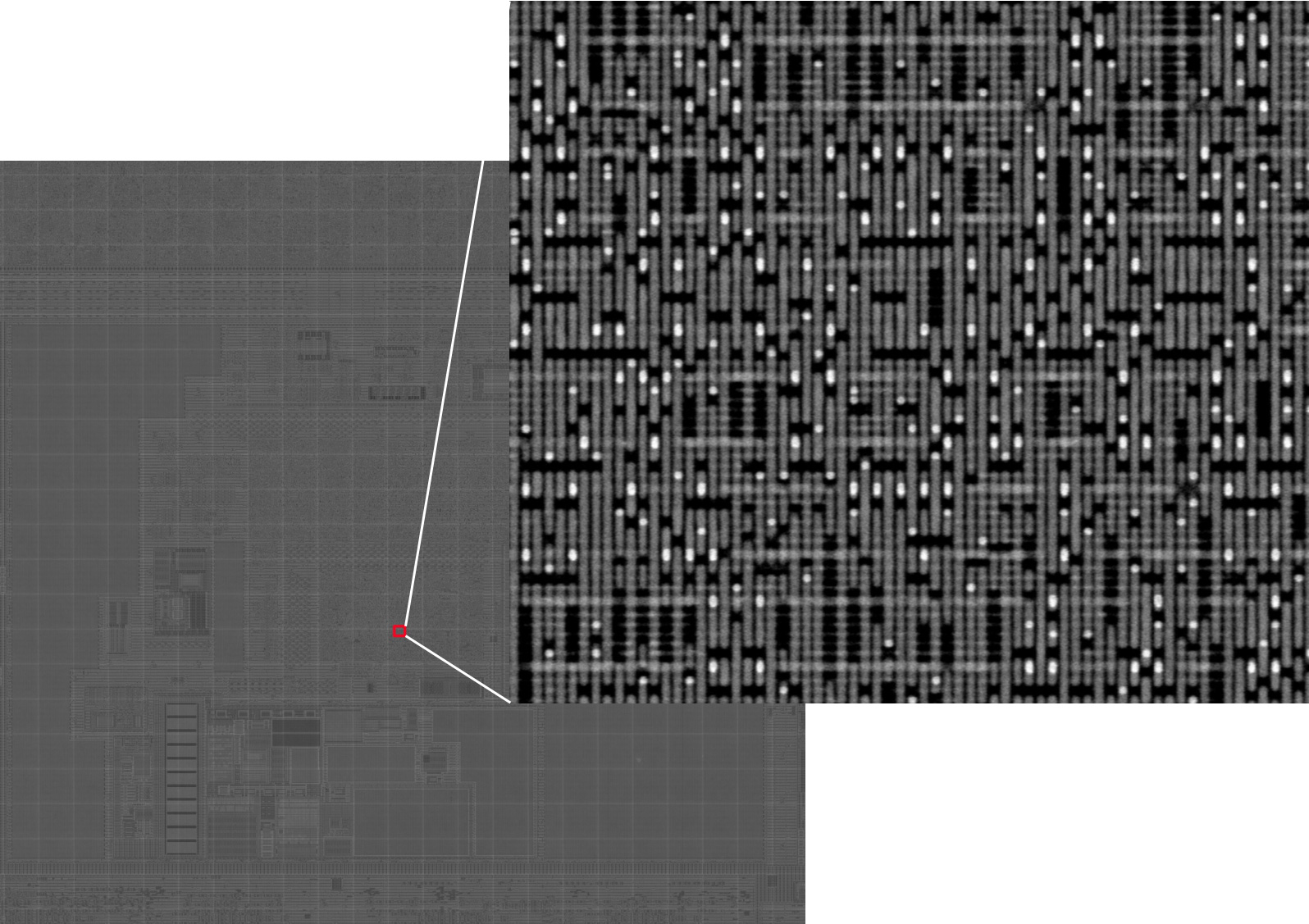
The CHIPSCANNER combines high-resolution electron optics, multiple high-efficiency electron detectors, and ultra-precise Laser Interferometer Stage technology with unique software to deliver homogenous large-area image mosaics for each layer with minimum stitching errors and stable brightness/contrast values and CAD shape extraction. With features such as
- Active focus control using laser height sensing
- Highest position and beam accuracy and stability, and
- A wide range of selectable electron detectors,
the CHIPSCANNER produces the most accurate large-area, high-resolution image mosaics directly acquired by an SEM instrument. Since the absolute position of each pixel, even over cm², is ultimately known to the accuracy provided by the laser interferometer stage and ultra-precise image calibrations, these images can be precisely stacked (3D-stitched).
Various high-speed detectors, flexible working distance, parallel detector stream handling and a high-speed scan generator allow precise and flexible image acquisition that is also high throughput.
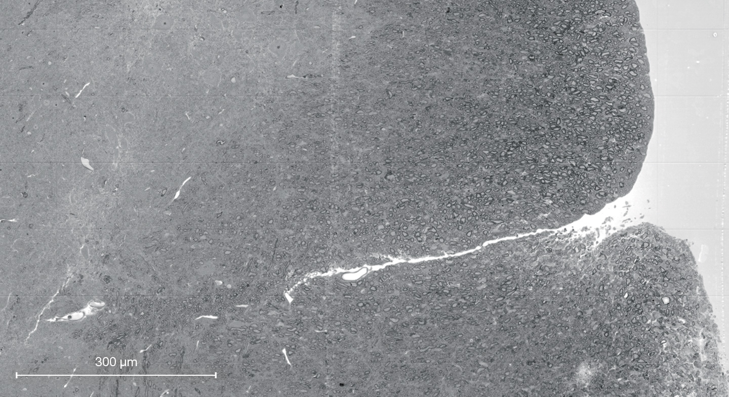
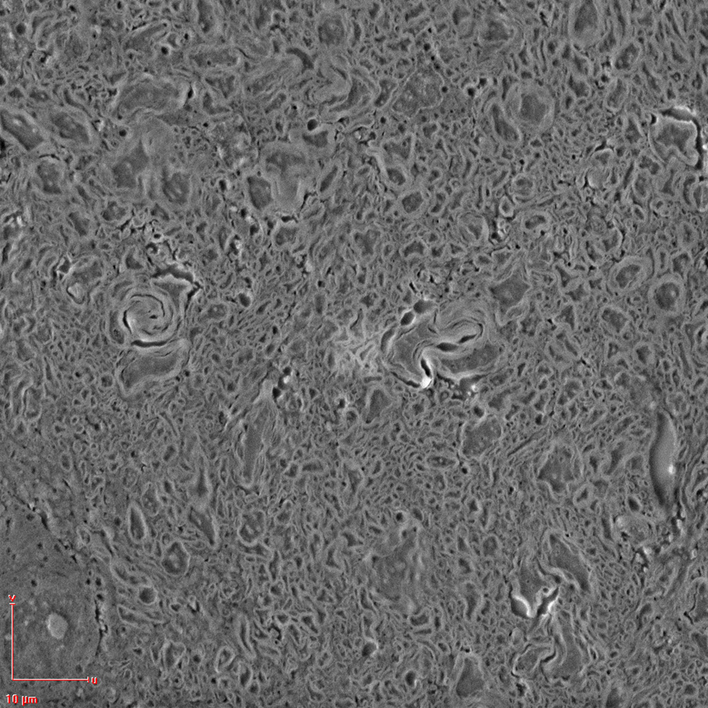
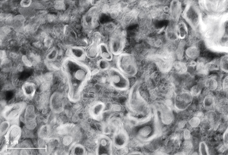
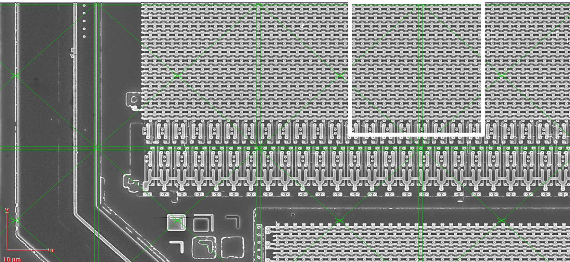
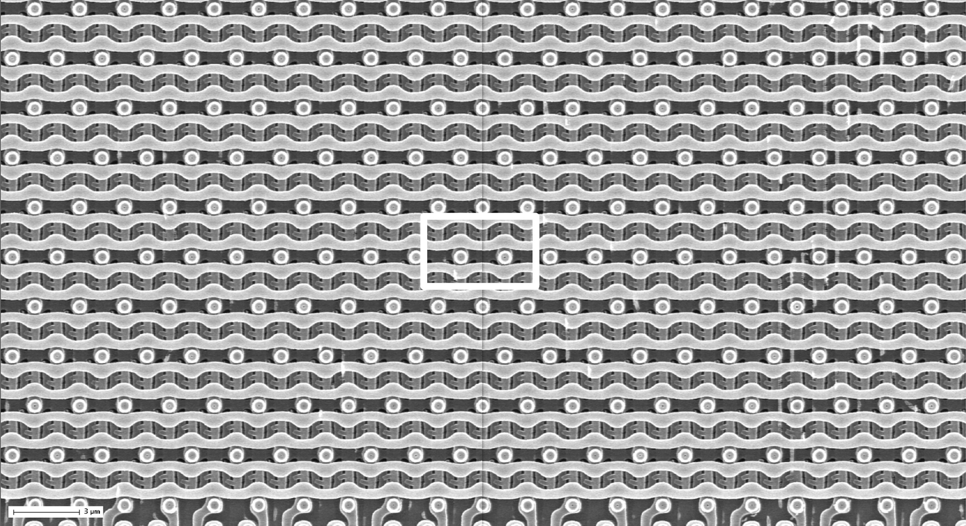
Large-area, ultra-high-resolution 3D SEM imaging applications in chip reverse engineering, materials science, and life sciences (e.g. connectomics) require surfaces of up to cm² areas to be scanned with nm resolution and excellent layer to layer accuracy (‘3D stitching’) for layout and schematic extraction or 3D modeling. While traditional SEM instruments are inherently limited by small, uncalibrated fields of view (FOVs) and imprecise sample positioning, the CHIPSCANNER addresses these challenges by combining the resolution and flexibility of an SEM instrument with the accuracy, stability, and automation of an electron beam lithography (EBL) instrument – a core area of expertise at Raith. High-resolution, large-area image mosaics are created by capturing sequential SEM images and stitching them together for further analysis, while the laser interferometer stage and field-of-view calibration reduce overlap to an absolute minimum and thus reduce required computing. A true large-area 3D SEM!
Data management for IC Analysis
Trojans, chip design recovery, spare parts supply, IP protection, and patent claim proofs are just a few of the many challenges the CHIPSCANNER helps to solve.
Originally designed for the demanding requirements and workloads that arise in the field of integrated circuit analysis , the CHIPSCANNER not only provides highest precision for accurate results. It also allows chips or any other sample to be scanned with nm resolution and excellent layer-to-layer accuracy for 3D models, layout, and optional netlist extraction. The extremely high volume of data can easily be handled in terms of both memory capacity and processing time. Software tools are available to process the images further to extract and optimize valuable CAD data (for mask generation or layout comparison).
Features
Calibrated single-image scans up to
50 k x 50 k pixel
2D mosaics up to
multiple cm²
Resolution down to
<1 nm
Simple workflow and intuitive GUI for easy adaptation of 3D SEM capabilties for science
A range of applications in materials sciences and life sciences can make use of the outstanding imaging capabilities originally designed for imaging semiconductor samples. The possible uses are manifold since the CHIPSCANNER is capable of delivering homogenous cm² large-image mosaics with nm resolution for any given substrate. The intuitive software with GUI simplifies the work and allows even users without EBL experience to use the system and achieve the desired results. Contact us to discuss your specific problem.


Raith Service - with you all the way
Specifications and system performance parameters are certainly drivers of decision-making where CHIPSCANNER is concerned. However, more factors need to be taken into consideration if efficient operation, continous uptime, and subsequent reliable support are to be ensured over the system’s lifetime.
With a worldwide team of professional service engineers, Raith Service ensures you can make the best use of your system. When you decide on a Raith system, all site surveys together with environmental measurements, support with the resulting cleanroom laboratory setup, factory and on-site acceptances, and comprehensive on-site training are always included. Moreover, application support is available free of charge in all global time zones.
Raith service contracts follow a modular scheme and can be configured to match your individual requirements and budget. Visit our Service site or get in touch with us to learn more.
Download CHIPSCANNER brochure
To find out more about the CHIPSCANNER, the possible applications and specifications
the whole CHIPSCANNER pdf package or the CHIPSCANNER product brochure